Low-pressure encapsulation for the protection of electronic assemblies
The hotmelt moulding process, also known as low-pressure encapsulation, has established itself in recent years as a cost-efficient and process-reliable alternative to conventional injection moulding and potting methods. Particularly for protecting and sealing electronic assemblies, the process offers decisive advantages in terms of component protection, flexibility, and cost structure.
Process principle
In hotmelt moulding, thermoplastic hotmelt materials – typically based on polyamides, polyolefins, or polyesters – are melted at processing temperatures of approximately 160 °C to 240 °C and injected into a tool at very low pressures, typically between 2 and 60 bar. By comparison, pressures in conventional plastic injection moulding are roughly 20 to 25 times higher.
Due to the low pressure and short thermal exposure time, the process is particularly suitable for sensitive components such as printed circuit boards, coils, sensors, or cable assemblies, which can be directly overmoulded. No chemical curing is required – the material solidifies purely through physical cooling.
Economic advantages
A key benefit of the hotmelt process lies in the low tooling costs. Because of the low process pressures, inexpensive aluminium moulds can be used, which can be manufactured quickly. This enables short development times and makes the process especially attractive for small to medium production volumes.
In addition, hotmelt materials offer low material costs, short cycle times, and a solvent-free processing method.
Protective function and design freedom
Hotmelt moulding provides reliable protection against:
- Moisture and dust
- Mechanical stress
- Electrical contact
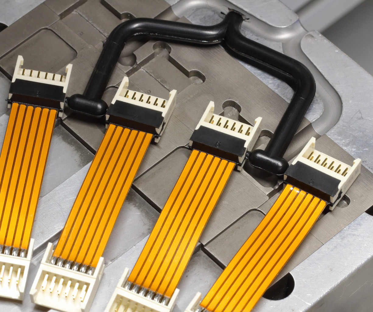
Depending on the design, protection ratings up to IP67/IP68 can be achieved. Both partial and full overmoulding are possible – from targeted encapsulation of individual components to complete housing replacement. Functional elements such as strain reliefs, bend protections, mounting features, or cable feedthroughs can also be directly moulded
Material properties
Hotmelt materials adhere to a wide range of substrates and are particularly suitable for porous or fibrous surfaces. Surface irregularities are compensated, while the adhesive joint remains elastic and simultaneously provides high sealing performance and tensile strength. The short-term thermal exposure of approximately 200 °C typically prevents damage to cable insulation or electronic components.
Typical Applications
- Cable grommets and bend protection
- Directly moulded strain reliefs
- Sealing of connectors
- Integration of electronics within cables
- Overmoulding of printed circuit boards
- Custom housings and feedthroughs
Hotmelt moulding represents a powerful, flexible, and economical solution for protecting electronic assemblies. Especially for small to medium production volumes, short development cycles, and sensitive components, low-pressure encapsulation offers clear advantages over conventional injection moulding or potting methods. Thanks to the wide variety of available materials and high design flexibility, the process has become firmly established in the electronics, automotive, and cable industries.